


PRODUCTS
How Do High-Sensitivity Geophones Protect Semiconductor Fabs from Micro-Vibrations?
In 2026, the semiconductor industry is operating at unimaginable scales. With foundries mass-producing sub-2-nanometer chips, the margin for error during the photolithography process has shrunk to the atomic level.
At these microscopic dimensions, an invisible and often overlooked enemy threatens multi-billion-dollar fabrication plants (fabs) every day: micro-vibrations.
Even the slightest seismic tremor, whether caused by a passing truck miles away, nearby ocean waves, or the HVAC systems of the fab itself, can misalign an Extreme Ultraviolet (EUV) lithography machine and ruin an entire batch of silicon wafers.
So, how do engineers detect and neutralize these imperceptible tremors? The answer lies in the physics and deployment of the high-sensitivity geophone.
Why Do Fabs Need Seismic Monitoring?
In traditional civil engineering, seismic monitoring is used to predict earthquakes or measure bedrock stability. In a semiconductor fab, however, the focus shifts to ambient seismic noise.
During the lithography process, light is used to print complex circuit patterns onto a silicon wafer. If the floor vibrates even a fraction of a micrometer, the pattern blurs.
This blurring causes structural defects in the microchips and drastically lowers the yield (the percentage of functional chips per wafer). Because high-end wafers can cost tens of thousands of dollars each, mitigating vibration is a top financial priority.
How Geophones Capture the Unseen
While standard industrial accelerometers are highly effective for measuring high-frequency machinery vibrations, they struggle to detect ultra-low-frequency vibrations (sub-1Hz to 10Hz) due to their inherent electrical noise floors.
High-sensitivity geophones solve this limitation by relying on the precise physics of electromagnetic induction and mass-spring dynamics.
Mechanically, a geophone acts as a damped harmonic oscillator. When an ambient seismic wave reaches the fab floor, the dynamic response of the internal proof mass can be described by the following differential equation:
mz¨+cz˙+kz=−mu¨
Here, m represents the proof mass, c is the mechanical damping coefficient, k is the spring stiffness, z is the relative displacement of the mass within the casing, and u¨ is the absolute ground acceleration caused by the micro-vibration.
As the ground moves, the relative velocity z˙ of the coil moving through the magnetic field generates an electromotive force (EMF) based on Faraday’s Law of Induction. The output voltage V(t) is directly proportional to the relative velocity:
V(t)=G·z˙(t)
In this equation, G is the intrinsic transduction constant of the geophone, often measured in V/m/s. Because this mechanism is entirely passive and self-generating, it offers an exceptionally low electrical noise floor. This allows the instrument to capture sub-micrometer waves that easily slip past standard digital sensors.
Deployment in the Cleanroom
In a modern semiconductor facility, these high-sensitivity instruments are deployed in two critical phases:
1. Site Surveying and Foundation Design
Before a fab is built, geotechnical engineers conduct a comprehensive micro-vibration survey of the land. They map out the power spectral density (PSD) of the vibrations within the bedrock. This data dictates the necessary thickness of the concrete foundation slabs (often referred to as “waffle slabs”) required to inherently dampen incoming waves according to stringent Vibration Criteria (VC) curves.
2. Active Vibration Isolation Systems (AVIS)
Inside the cleanroom, EUV lithography machines do not sit directly on the floor; they rest on Active Vibration Isolation Systems. High-sensitivity geophones are installed directly on the facility floor and the machine pedestals to act as the primary feedback loop.
When a geophone detects an incoming micro-vibration, the recorded voltage is fed into a real-time digital signal processor. The system calculates the required counter-force Fcontrol needed to cancel the movement using a closed-loop feedback algorithm, typically incorporating proportional-derivative control:
Fcontrol(t)=-(Kpzerror+Kdz˙error)
Electromagnetic actuators then instantly apply this force to the machine pedestal, effectively canceling out the tremor before the kinetic energy can transfer to the silicon wafer.
Equipping Fabs for the Future
Because the tolerance for vibration in sub-2nm manufacturing is virtually zero, facility managers cannot compromise on sensor precision. Instruments deployed in these environments must feature ultra-low distortion, superior spurious frequency limits, and absolute continuous reliability.
When designing sophisticated vibration monitoring architectures for advanced cleanrooms, engineers turn to proven precision instruments. By integrating high-sensitivity geophones and seismic sensors into their active cancellation systems, semiconductor foundries can ensure their lithography tools remain perfectly still.
High-quality sensors provide the crystal-clear, low-noise voltage signals required to keep automated isolation loops reacting flawlessly.
Conclusion
As the global demand for faster, smaller, and more powerful microchips continues to surge, the environments they are built in must become increasingly controlled. The high-sensitivity geophone might have its roots in geological exploration, but today, its underlying physics makes it an absolute necessity in the semiconductor field.
By translating the faintest mechanical tremors into precise electrical signals, geophones safeguard the fundamental manufacturing technology that powers our modern world.
Related Products
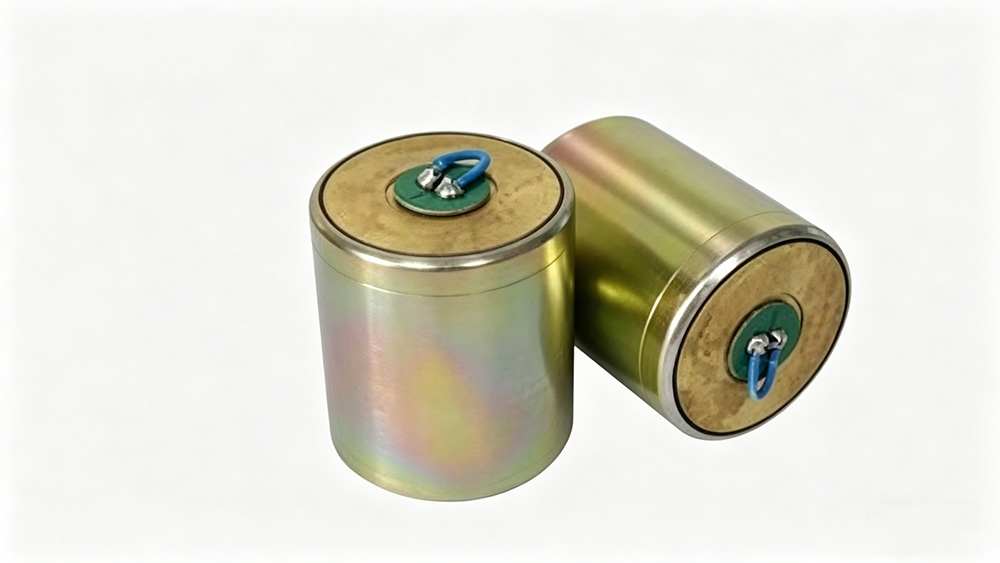
- High sensitivity geophone 2Hz:
- High sensitivity geophone 1Hz:
References
- Gordon, C. G. (1991). Generic Criteria for Vibration-Sensitive Equipment. Proceedings of SPIE 1619, Vibration Control in Microelectronics, Optics, and Metrology.
- Amick, H., Gendreau, M., Busch, T., & Gordon, C. (2005). Evolving criteria for research facilities: I-Vibration. Proceedings of SPIE.
- Technical Manufacturing Corporation (TMC). (n.d.). Active Vibration Isolation Systems. Retrieved from TMC Technical Background.
- Ryaboy, C. B. (2024). Vibration Control Solutions for Microscopy. Technical Manufacturing Corporation (TMC) / AMETEK.
- Lee, J. H., et al. (2024). An Active Geophone Sensor with Optimized State Variable Filter for Measuring Low-Band Frequencies. ResearchGate.
- IMV Corporation. (n.d.). Broad Motion Sensor VP-8013 / VP-8013S for Micro Vibration Measurement. IMV Technical Documentation.

For any inquiries, please contact with our Marketing Team at sales@seis-tech.com or Supporting Team at info@seis-tech.com.
 MAIN TECHNICAL PARAMETERS
 Related products


